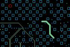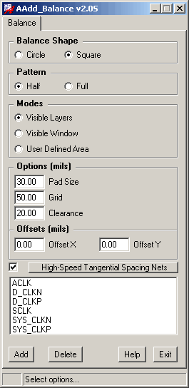
BALANCE PADS (aka Theiving pads) to any
copper layer or by a user defined area.
• User can select visible layers, visible window
or 2-point pick area to add copper-balance
pads.
• Copper-balance pads can be either Square
or Circle shaped.
• User has control of the copper-balance size,
grid and clearance to other copper features.
• The pattern for pad placement set to full or
half (checker board) patterns.
• Pads will not be added inside the perimeter
of any solder resist opening.
• Tangential spacing for high speed nets
to adjacent layers.